If you’ve ever worked with power cables, you’ve probably heard the terms “inner semicon” and “outer semicon” tossed around, but do you actually know what sets them apart? As someone who’s been supplying power cable compounds for over a decade—jumping on calls with utility engineers, troubleshooting line issues, and tweaking formulations to fit real-world grid needs—I can tell you this isn’t just a technical fine print. Mix these two up, and you’re looking at premature cable failure, hot spots, or even power outages that cost companies thousands. Let’s break this down like we chat on a Monday morning, no stuffy lab jargon that makes your eyes glaze over. Power Cable Compounds
First, let’s start with the basics: semiconductive compounds aren’t insulators, but they aren’t conductors either—they sit in that weird “middle” zone that makes power cables work. A standard high-voltage power cable (think the ones strung on utility poles or buried under cities) has three core layers stacked like a sandwich: a copper or aluminum conductor down the middle, an insulation layer around that, and a protective jacket on the outside. If you just left bare metal touching the insulation, you get something called “partial discharge”—little sparks that eat away at the insulation over time, eventually leading to a blowout. That’s where the two semicon layers come in, but they’re not doing the same job.
Inner semicon’s whole gig is sticking directly to the conductor, right where the metal meets the insulation. Imagine the conductor is a bumpy road—all those tiny metal nooks and crannies would create air gaps between the metal and insulation. Those gaps act like little pressure cookers for electrical stress, leading to partial discharges. Inner semicon is designed to fill in every crevice, smoothing that metal surface so the insulation and conductor are totally smooth, no gaps. It’s also engineered to carry a tiny, negligible current—just enough to keep electrical stress even, no more. If inner semicon was too conductive, it would bleed power unnecessarily; if it was too resistive, those gaps come back. The magic here is balancing that resistance: inner semicon typically has a volume resistivity of 10² to 10⁴ ohm-centimeters—way lower than insulation (which is 10¹² ohm-cm or higher) but way higher than pure copper (which is like 10⁻⁶ ohm-cm).
Outer semicon’s job, on the other hand, is the opposite of inner semicon. It wraps around the outside of the insulation, not the conductor, and it’s meant to connect to the ground system—whether that’s a metal sheath around the cable, the earth itself, or a grounded grid component. Instead of smoothing the inside, outer semicon is creating a low-resistance path to siphon off any electrical stress that builds up in the insulation. Think of it like a lightning rod for the cable: stray current gets pulled to the outer semicon, then to ground, instead of wandering into the insulation and causing damage. Its resistivity is a little higher than inner semicon, usually around 10⁴ to 10⁶ ohm-cm, but the key difference is what it’s touching and who it’s paired with.
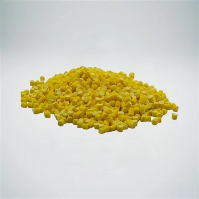
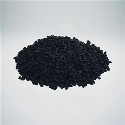
Wait, let’s get into how they’re made too—because that’s a big part of why they act differently. Most power cable compounds are cross-linked polyethylene (XLPE) based, since XLPE is the go-to insulation for high-voltage cables. Inner semicon gets loaded with carbon black—super fine, conductive carbon particles—at just the right concentration. Too much carbon, and it’s too conductive, leaking power; too little, and it can’t smooth the conductor surface. We test ours in-house all the time: adjust the carbon loading by 0.5% and resistivity changes by a whole order of magnitude. Outer semicon is also carbon black filled, but sometimes with a slightly different grade of carbon to get that tiny boost in resistivity it needs. Also, outer semicon often has a tiny amount of a cross-linking retarder—something we add in our formulations to make sure it doesn’t cross-link too early when it’s being extruded onto the cable. If outer semicon cross-links prematurely, it can peel off the insulation, leaving gaps where stress can build up. Inner semicon doesn’t need that retarder because it’s bonded directly to the conductor, so cross-linking is a good thing there—it makes the layer tough enough to stay stuck.
Another big difference: how they interact with the cable’s installation and lifespan. Inner semicon is a permanent bond—when you extrude it onto the hot conductor, it cross-links right there, fusing to both the metal and the insulation layer. That bond is non-negotiable; if it peels, you’ve got a catastrophic risk. Outer semicon, though, often has a very thin layer of insulation between it and the metal sheath, or it’s just in contact with the grounded sheath. If outer semicon gets damaged during installation (say, a construction crew nicks the cable jacket and scrapes the outer semicon), it can be repaired with a special tape—no need to re-extrude the whole thing. Inner semicon damage is way trickier; you can’t just patch a conductor gap, you have to re-extrude the entire inner semicon layer, which adds time and cost to a repair job.
Let’s talk real-world examples to make this concrete. Last year, we worked with a utility in the Midwest that was having constant cable failures on their 138kV lines. They thought the insulation was bad, but when we ran tests, it turned out their outer semicon was too resistive. The outer semicon couldn’t pull stress to ground, so that stress built up until it punctured the insulation. We swapped their outer semicon compound for our grade optimized for 138kV lines, and their failure rate dropped by 70% in 12 months. Another time, a cable manufacturer was having issues with inner semicon peeling off the conductor during extrusion—turns out they were using a carbon black with too large a particle size, and it wasn’t bonding well. We recommended a finer carbon grade, and that fixed their line defect rate.
Now, let’s clear up a common myth: people sometimes say “semicon is just semicon,” but that’s like saying all glue is the same—you wouldn’t use wood glue on a ceramic mug, same logic applies. Inner and outer aren’t interchangeable; using outer semicon where inner goes would leave huge gaps, and using inner semicon where outer goes would bleed too much power, leading to energy loss and overheating. Also, they’re not just for high-voltage cables—low-voltage power cables (like the ones in buildings) have thinner semicon layers, but the same basic design rules apply.
So, when you’re sourcing power cable compounds, what should you be looking for? First, make sure your supplier can distinguish between the two, and can tailor formulations to your voltage class. A lot of suppliers sell a generic semicon that works okay for one, but not both. At our company, we test every batch: check resistivity with a four-point probe to make sure inner is in that 10²-10⁴ range, outer is 10⁴-10⁶. We also run heat aging tests—put samples in an oven for 1000 hours at 130°C, make sure resistivity doesn’t shift more than 10%. Because if the resistivity shifts after a few years of being in the ground, that’s when problems start.
At the end of the day, inner and outer semicon are two sides of the same coin—inner smooths the inside to keep stress from building up at the conductor, outer dissipates stress to ground to keep the insulation safe. Mix them up, and you’re looking at avoidable downtime and costs. If you’re working on a cable project, troubleshooting a recurring failure, or just updating your compound spec and need to make sure you’re picking the right semicon for inner vs. outer, feel free to reach out to our team to chat through your needs. We can send you test data, adjust formulations for your voltage class, or help you figure out where your current process might be slipping up. Don’t waste time guessing—let’s talk through it.
Communication Cable Compounds References
- Nelson, J. K. (2013). Dielectric Phenomena in High Voltage Engineering. Wiley-IEEE Press.
- Kreuger, F. H. (1991). Partial Discharge in Electrical Equipment. Delft University Press.
- IEEE Std 404™-2018, Standard for Extruded Cross-Linked Polyethylene (XLPE) Insulated Power Cables for Rated Voltages 5 kV through 345 kV.
Opta New Materials (Jiangsu) Co., Ltd.
As one of the most professional power cable compounds manufacturers and suppliers in China, we also support customized service. We warmly welcome you to buy bulk durable power cable compounds from our factory. If you have any enquiry about free sample, please feel free to email us.
Address: No.80, Jingang Avenue, Zhenjiang New Area, Zhenjiang City, Jiangsu Province, China.
E-mail: le.yin@optachem.com
WebSite: https://www.optanewmaterials.com/
